Benefits Include Increased Performance, Reduced Power Needs and Enhanced Miniaturization
The global 3D IC (three-dimensional integrated circuit) market will reach a value of $22.30 Billion by 2027. The increasing demands for smart devices and the importance of miniaturization in the electronics industry are influencing the market growth.
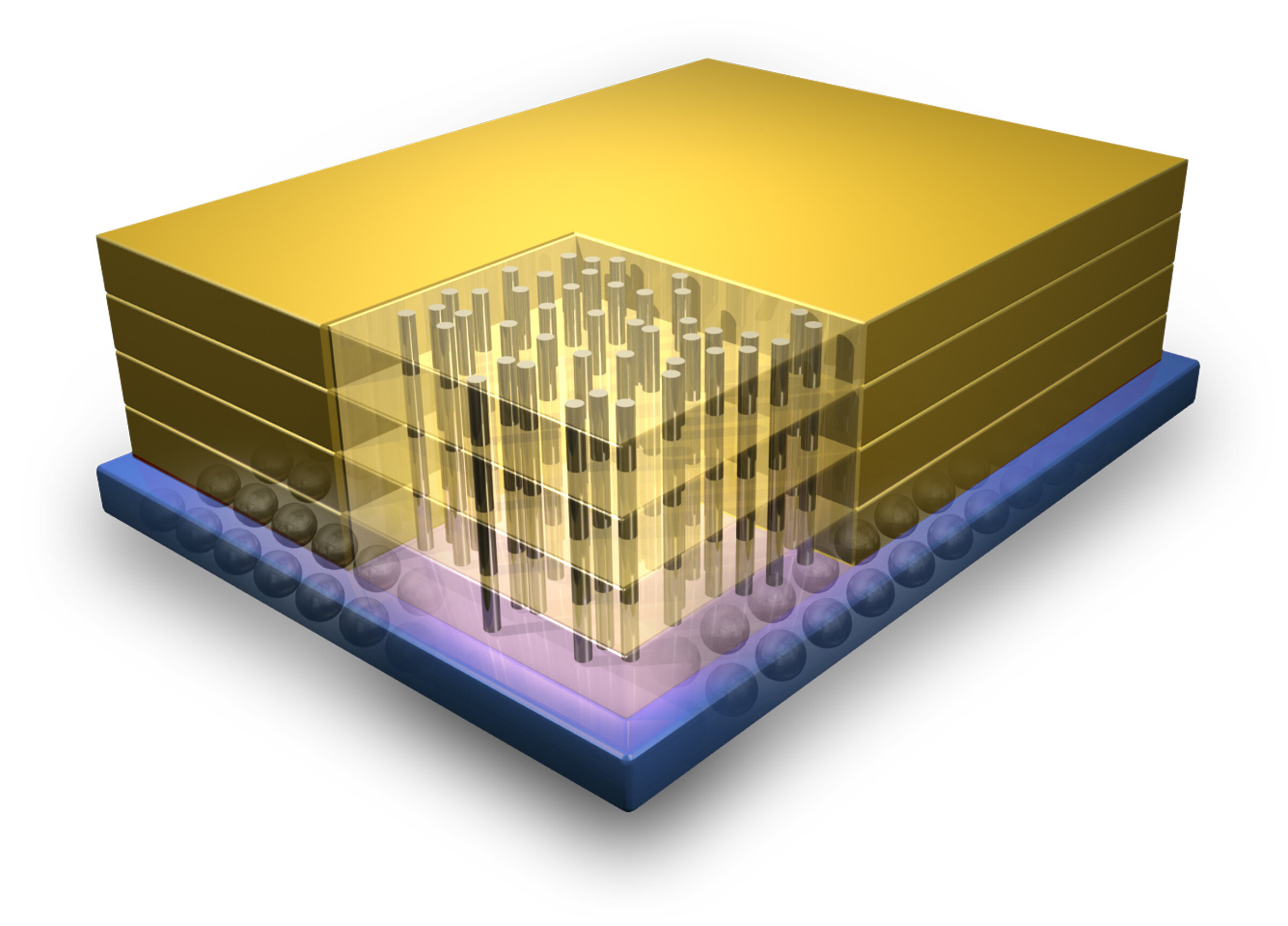
As it's become more difficult to shrink existing processes, stacking up is the way to increase integration. Stacking can be done die-on-die, die-on-wafer, wafer-on-wafer, or in combination. A 3D IC is a MOS (metal-oxide-semiconductor) integrated circuit (IC) manufactured by stacking silicon wafers or dies and interconnecting them vertically using, for instance, through-silicon vias (TSVs) or Cu-Cu connections, so that they behave as a single device. (Wikipedia, 2021)
3D ICs not only improve the performance and functionality of electronic devices, but they also allow the integration of disparate technologies such as logic, memory, RF, sensors, optical components etc. in small form factors. The small size of 3D ICs is valuable in miniaturized devices, such as smartphones, implantable devices and IoT applications.
Industries able to bear the higher cost of 3D integration technologies, such as Automotive, Consumer electronics, Medical devices, Military & Aerospace, Telecommunication, Industrial sector, and smart technologies, are driving the technology. 3D ICs are considered an optimum solution for devices that require a large storage capacity and bandwidth.
The benefits of 3D IC include:
Reduced Footprint
Stacking multiple dies atop one another produces a chip that takes up less space than if those dies were side by side: a multi-layer 3D-IC is no thicker than a traditional 2D chip.
Speed
The shorter distance of dies stacked in a 3D chip is much closer together than chips on a circuit board, allowing electronic signals to travel more quickly from one component to another, increasing speed fivefold.
Power
The shorter connections require less power. Another power-saving aspect is that signals that travel from one layer to another within a 3DIC do not require ESD checks (ESD filters consume energy), reducing power consumption up to 90%.
Heterogeneous Integration
Because the layers in a 3D IC are manufactured separately, they can be built differently, affecting the cost, complexity, and performance of each layer. A 3D IC can combine the best of each process, node, and substrate without compromising some components to accommodate others. Circuit layers can be built with different processes, or even on different types of wafers. Components with incompatible manufacturing could be combined in a single 3D IC. So distinct technologies, comprising memory and logic circuits, mixed-signal and radio frequency (RF) components, and optoelectronic devices, etc. can be combined on different dies of a 3D IC.
There are hurdles to overcome. These include:
Cost
3D ICs have a higher cost per unit than traditional alternatives in mainstream consumer applications. As the technology is adopted, these costs will be reduced.
Yield
Each extra manufacturing step adds a risk for defects.
Heat
Heat building up within the stack must be dissipated. Heat increases when electrical proximity correlates with thermal proximity.
Manufacturing Complexity
The manufacturing steps must be carefully coordinated if different layers are processed by different manufacturers, and they are stacked at yet another facility.
In specific markets such as memories and sensors, the immediate benefits of 3D far outweigh the difficulties as well as in markets such as the consumer electronics market that is trying to enhance the user experience as well as pursuing device miniaturization.
The consumer electronics market is looking to 3D ICs to overcome challenges with enhancing performance and lowering power consumption while reducing chip size.
The global 3D IC market has very few vendors at present, with the top players in the market dominating the market. Top vendors for 3D IC market are:
Advanced Semiconductor Engineering
ASE is one of the pioneers in 2.5D/3D packaging technology and has successfully introduced the mass production of the world's first 2.5D IC package equipped with High Bandwidth Memory (HBM). (2.5D refers to die stacking package using interposers to achieve the best performance of internet connectivity.) Integrating GPU, CPU, and memory together with decoupling capacitor is feasible by ASE 2.5D IC solution.
Intel
Intel has launched its first heterogeneous chip architecture made using its Foveros 3D chip stacking technology, combining a 10nm HPC chiplet with a low-energy 22nm base die and stacked with memory on top.
Samsung Electronics
Samsung's X-Cube test chip is built on 7nm using TSV technology to stack SRAM on top of a logic die, the ultra-thin package design features significantly shorter signal paths between the dies for maximized data transfer speed and energy efficiency. Customers can also scale the memory bandwidth and density to their desired specifications.
Taiwan Semiconductor Manufacturing
TSMC is one of the leading vendors in the global 3D IC market as well as in the global semiconductor foundry market. The company offers a wide range of integrated semiconductor foundry services that focus on increasing customer needs. TSMC is the first company to have 40 nm and 60 nm production capacity. TSMC is looking to commercialize its SoIC (system on integrated chips) technology for 3D heterogeneous integration in 2021.
Xilinx
Xilinx UltraScale 3D ICs provides unprecedented levels of system integration, performance, bandwidth, and capability. Both Virtex® UltraScale 3D ICs and Kintex® UltraScale 3D ICs contain a step-function increase in both the number of connectivity resources and the associated inter-die bandwidth in this second-generation 3D IC architecture.